
AMD/Xilinx XC6SLX100-2FG676C FPGAs (Field Programmable Gate Array)
IC FPGA 480 I/O 676FCBGA
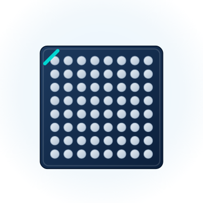
Same model may have multiple batches, images only for reference.
Technical Specifications
AMD/Xilinx XC6SLX100-2FG676C FPGAs (Field Programmable Gate Array) technical specifications.
General
Related Parts Comparison (XC6SLX100-2FG676C vs XC6SLX100-3CSG484I vs XC6SLX100T-3FGG484I vs XC6SLX100T-2FGG484I)
Side-by-side specifications of related catalog parts.
Engineering verification required. Related parts may have different electrical ratings, pinouts, footprints, and operating limits. Verify suitability for your circuit before substitution.
| This Part | Related Part | Related Part | Related Part | |
|---|---|---|---|---|
| Package / Case | 676-BGA | 484-FBGA | 484-BBGA | 484-BBGA |
| Mounting Type | Surface Mount | Surface Mount | Surface Mount | Surface Mount |
| Operating Temperature | 0°C ~ 85°C (TJ) | -40°C ~ 100°C (TJ) | -40°C ~ 100°C (TJ) | -40°C ~ 100°C (TJ) |
| Supply Voltage | 1.14V ~ 1.26V | 1.14V ~ 1.26V | 1.14V ~ 1.26V | 1.14V ~ 1.26V |
| RoHS | No | Yes | Yes | Yes |
| Lifecycle Status | Active | Active | Active | Active |
| Number of I/O | 480 | 338 | 296 | 296 |
| Number of LABs/CLBs | 7911 | 7911 | 7911 | 7911 |
| Number of Logic Elements Cells | 101261 | 101261 | 101261 | 101261 |
| Package | FBGA | 484-FBGA, CSPBGA | FBGA | FBGA |
| Total RAM Bits | 4939776 | 4939776 | 4939776 | 4939776 |
| Number of Pins | 676 | -- | 484 | 484 |
| Action |
AMD/Xilinx XC6SLX100-2FG676C FPGAs (Field Programmable Gate Array) Overview
Field Programmable Gate Array (FPGA) with 101,261 logic cells and 126,576 registers, built on 45nm process technology. Features 480 user I/Os, 4824 Kbit RAM, and 360 18x18 multipliers. Operates at 1.2V with a transceiver speed of 3.2 Gbps. Packaged in a 676-pin Fine Pitch Ball Grid Array (FBGA) for surface mounting, with dimensions of 27mm x 27mm x 1.73mm.
More Parts in FPGAs (Field Programmable Gate Array)
XC6SLX100-L1FGG676CAMD/Xilinx